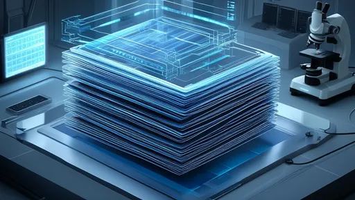
The world of electronics stands on the cusp of a transformative era, driven not by the refinement of old architectures but by the emergence of entirely new material systems. At the forefront of this revolution are two-dimensional (2D) materials and, more critically, the sophisticated structures built from them: van der Waals heterostructures. These are not merely new substances to be plugged into existing silicon paradigms; they represent a fundamental redesign of the very platform upon which future electronic, optoelectronic, and quantum devices will be built. By stacking atomically thin layers like graphene, transition metal dichalcogenides (TMDs), and hexagonal boron nitride (hBN) with deliberate precision, scientists are crafting a designer's playground with unprecedented control over material properties.
The magic of these heterostructures lies in the van der Waals force—the same weak, attractive interaction that allows a gecko to walk up a wall. This force enables the stacking of different 2D crystals without the stringent need for perfect lattice matching, a fundamental and often crippling requirement in traditional semiconductor epitaxy. This liberation from lattice constraints is monumental. It allows researchers to combine materials that were previously incompatible, creating hybrid systems with properties that are not just the sum of their parts, but entirely new and emergent phenomena. The interface is everything; it becomes the active, functional heart of the device, governing charge transport, light-matter interaction, and spin dynamics.
One of the most direct and impactful applications of this platform is in the realm of tunneling devices. By sandwiching a semiconductor TMD, such as molybdenum disulfide (MoS₂), between two layers of graphene, a vertical tunnel field-effect transistor (TFET) can be created. Unlike conventional transistors that rely on the thermal injection of charge carriers over a barrier, TFETs operate on the principle of quantum mechanical tunneling through the barrier. This allows them to switch on and off with a much steeper subthreshold slope, potentially operating at voltages below 0.1 volts. The atomically sharp interface in a van der Waals heterostructure is the perfect embodiment of an ideal tunnel junction, minimizing defects and trap states that plague traditional attempts at building TFETs. This paves the way for a new generation of ultra-low-power electronics, a critical need for the ever-expanding Internet of Things (IoT).
Beyond tunneling, the heterostructure platform is breathing new life into the concept of the p-n junction, the fundamental building block of modern electronics and optoelectronics. Traditionally, creating a p-n junction involves the complex and aggressive process of doping a single semiconductor crystal with different impurities. In the 2D world, a junction can be formed far more elegantly by simply placing a p-type 2D semiconductor (like WSe₂) on top of an n-type one (like MoS₂). The resulting van der Waals p-n junction is atomically sharp and free from the lattice disorder inherent to chemical doping. These junctions exhibit exceptional photovoltaic responses and electroluminescence, making them ideal for ultra-thin, flexible, and highly efficient light-emitting diodes (LEDs) and photodetectors. Their performance can be further tuned by applying gate voltages, creating dynamically reconfigurable optoelectronic circuits.
Perhaps the most exciting frontier is the use of these heterostructures to create and manipulate exotic quantum states of matter. When two graphene layers are stacked at a specific "magic angle" of approximately 1.1 degrees, the resulting moiré pattern dramatically alters the electronic landscape. This twist engineering creates flat bands in the electronic structure, where electron interactions become dominant, leading to the emergence of strongly correlated states like superconductivity and Mott insulation. This discovery of twistronics has opened a vast new field where the electronic properties of a device are not defined by the chemical composition of the materials alone, but by the geometric angle between them. It provides a powerful new knob to turn, enabling the on-demand design of quantum materials for advanced computing and fundamental physics exploration.
The design flexibility extends to creating pristine environments for delicate quantum phenomena. A layer of semiconducting TMD can be encapsulated between two inert layers of hexagonal boron nitride (hBN), which has an atomically smooth surface and no dangling bonds. This encapsulation shields the sensitive TMD from disruptive environmental disorder, allowing its intrinsic quantum properties, such as tightly bound excitons and single-photon emission, to flourish at higher temperatures. This is not just an improvement; it is a necessary step towards practical quantum information processing and novel valleytronic devices, where information is encoded in the quantum valley degree of freedom of electrons.
Despite the breathtaking progress, the path from laboratory wonder to commercial technology is fraught with challenges. The synthesis of large-area, high-quality 2D crystals remains a complex and costly endeavor. The assembly of these layers into complex heterostructures, while advanced through techniques like deterministic pick-and-place transfer, is still a painstakingly slow and manual process ill-suited for mass production. New methods, such as direct growth of stacked heterostructures or wafer-scale transfer techniques, are under intense investigation but are not yet mature. Furthermore, the long-term stability and reliability of these atomically thin devices under real-world operating conditions require thorough investigation.
Nevertheless, the research community is tackling these hurdles with relentless innovation. The potential payoff is too significant to ignore. Van der Waals heterostructures are more than just a new class of materials; they represent a new philosophy in materials design—one of assembly and customization. This platform empowers scientists to act as architects, designing the electronic and optical landscape of a device from the ground up, atom by atom, interface by interface. It is a platform that promises not just incremental improvements, but the foundational technology for a future of flexible, transparent, ultra-low-power, and quantum-ready electronics. The journey of discovery is far from over, but the blueprint for the next generation of electronic devices is being drawn, one two-dimensional layer at a time.

By /Aug 25, 2025

By /Aug 25, 2025
By /Aug 25, 2025

By /Aug 25, 2025
By /Aug 25, 2025

By /Aug 25, 2025

By /Aug 25, 2025

By /Aug 25, 2025
By /Aug 25, 2025
By /Aug 25, 2025
By /Aug 25, 2025

By /Aug 25, 2025

By /Aug 25, 2025
By /Aug 25, 2025

By /Aug 25, 2025

By /Aug 25, 2025

By /Aug 25, 2025

By /Aug 25, 2025
By /Aug 25, 2025
By /Aug 25, 2025